


Next: EEL6935: HW#4
Up: EEL6935: Homework Assignments
Previous: EEL6935: HW#2
Get PDF file
EEL 6935: HW#3 REVISED
Due Friday, November 1, 2002 in class. Late homework loses
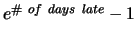 percentage points. See
the current late penalty at http://www.cnel.ufl.edu/hybrid/harris/latepoints.html
percentage points. See
the current late penalty at http://www.cnel.ufl.edu/hybrid/harris/latepoints.html
- 1.
- Solve for
 as a function of the difference of the two input voltages (
 ) for below threshold CMOS
operation. As usual, first, assume
) for below threshold CMOS
operation. As usual, first, assume  and derive your answer. Then assume
  is the same for all
transistors but not equal to one and derive your answer. Simplify your expressions as much as possible. Show all of
your work and explicitly state all assumptions, e.g. which transistors are in saturation, subthreshold operation,
matching of devices, etc.
is the same for all
transistors but not equal to one and derive your answer. Simplify your expressions as much as possible. Show all of
your work and explicitly state all assumptions, e.g. which transistors are in saturation, subthreshold operation,
matching of devices, etc.
- 2.
- Solve for as a function of the difference of the two input voltages () for below threshold CMOS
operation. As usual, first, assume and derive your answer. Then assume is the same for all
transistors but not equal to one and derive your answer. Simplify your expressions as much as possible. Show all of
your work and explicitly state all assumptions, e.g. which transistors are in saturation, subthreshold operation,
matching of devices, etc.
- 3.
- Solve for as a function of
 and
and  for the 5-transistor transamp in the above-threshold region.
Develop a defintion to quantify the width of the ``linear region'' of this curve. Come up with an approximate
expression for the width of the linear region as a function of the above threshold bias voltage. What is the exact
linear region width for the below threshold transamp according to your definition?
for the 5-transistor transamp in the above-threshold region.
Develop a defintion to quantify the width of the ``linear region'' of this curve. Come up with an approximate
expression for the width of the linear region as a function of the above threshold bias voltage. What is the exact
linear region width for the below threshold transamp according to your definition?
- 4.
- Explain the operation of the inner hair cell circuit in Fig. 1.9 of the cochlea paper by Sarpeshkar, Lyon and Mead.
Could a simple inverter be used instead of transistors BA and PA to charge and discharge the capacitor
 ?
Explain why or why not.
?
Explain why or why not.
- 5.
- Use a VLSI design system of your choice (e.g. CADENCE and layout a simple 5-transistor tranconductance
amplifier in the 0.6um AMI technology.). Make all of your transistors 6
 by 6 except for current
mirror transistors which should have a longer length of 20. Make sure that you have well and substrate
contacts. If possible, use software to verify that your layout is identical to a schematic or netlist that you
create. You only need to turn in a plot of your layout.
by 6 except for current
mirror transistors which should have a longer length of 20. Make sure that you have well and substrate
contacts. If possible, use software to verify that your layout is identical to a schematic or netlist that you
create. You only need to turn in a plot of your layout.
Next: EEL6935: HW#4
Up: EEL6935: Homework Assignments
Previous: EEL6935: HW#2
Dr John Harris
2002-12-02
![\includegraphics[scale=0.75]{/home/users/harris/classes/6935/hw3/bump.eps}](img28.gif)
![\includegraphics[scale=0.75]{/home/users/harris/classes/6935/hw3/diodes.eps}](img29.gif)